
A lithography machine is a projection exposure system primarily used insemiconductor chip manufacturing to transfer circuit patterns from a photomaskonto a silicon wafer coated with photoresist. It is one of the core pieces ofequipment in integrated circuit fabrication. The machine uses an optical systemto precisely project the mask's circuit design onto the wafer. Through theprocesses of photoresist exposure and development, the initial circuit patternis formed.
Often referred to as "the most precise machine ever built," the semiconductor lithography machine is among the most critical tools in chipproduction. Its technological sophistication directly determines the level ofrefinement achievable in chip manufacturing.
Lithography equipment accounts for the largest market share amongsemiconductor manufacturing tools. Among the key equipmentcategories—lithography machines, etching tools, and thin-film depositionsystems—lithography alone makes up 24% of the market. This share continues togrow with each new generation of chip processing nodes.
The development of semiconductor lithography wavelengths has undergoneseveral stages: from early 365nm mercury lamps, to 248nm krypton-fluoridelasers in the late 1990s, and then to 193nm argon-fluoride lasers in the early2000s. As the 193nm wavelength approached its physical limits, immersionlithography emerged around 2006, using water between the lens and wafer toincrease the numerical aperture from 0.93 to 1.35, establishing 193nm immersionlithography as the mainstream technology.
However, as chip integration and performance requirements continue torise, traditional lithography has once again neared its physical boundary.Extreme Ultraviolet (EUV) lithography, using a 13.5nm wavelength, has becomethe key to breaking through this limit. Developed by ASML, EUV lithography nowsupports 7nm and even more advanced nodes. It is regarded as a coretechnological breakthrough to extend Moore’s Law and is propelling thesemiconductor industry into the next era of innovation.
The following is a roadmap for the development of lithography machinestowards higher resolution technology:

Market Overview:
According to LookWhole Insight, the global LithographyEquipment market is projected to reach USD 27.27 Billion in 2024. It isexpected to grow to USD 51.41 Billion by 2033, registering a compound annualgrowth rate (CAGR) of 7.65% during the forecast period (2025–2033). - LookWhole Insight

Key Development Trends
1. AIDriving Demand
AI applications arefueling demand for advanced logic chips and high-end memory products—especiallyinference/training chips for AI servers. In other industries, emergingtechnologies and growing demand are also driving continual fab expansion andincreased investment in lithography and related semiconductor equipment.
ASML forecasts thatservers, data centers, and storage will be the primary beneficiaries in theearly stages of AI industry development. By 2030, related semiconductor salesare expected to exceed USD 350 billion, with AI servers (fortraining/inference) being a major growth driver due to their high chip content.Other fields such as smartphones, automotive electronics, and industrialelectronics are expected to grow steadily. Automotive semiconductor sales aloneare projected to reach USD 112 billion by 2030 (from USD 70 billion in 2025).ASML also anticipates additional capacity expansion driven by supply chainsecurity and national strategic considerations.

2. China’sPush for Localization
Since2018, the U.S. has been pressuring restrictions on high-end lithographyequipment exports to China, gradually escalating with measures such as the“1007 rule,” and working with Japan and the Netherlands to enforce joint exportcontrols—effectively tightening the blockade on China’s semiconductor industry.In response, domestic substitution of critical equipment like lithographymachines has become increasingly urgent.
In2016, Shanghai Micro Electronics Equipment (SMEE) successfully delivered itsSSA600 ArF lithography machine for the 90nm node. In 2020, Huazhuo Precisionbroke ASML’s monopoly on lithography wafer stage technology. In 2025, HarbinInstitute of Technology announced a breakthrough in developing a 13.5nm EUVlight source—an important milestone in light source technology. Additionally,the Shanghai Institute of Optics and Fine Mechanics under the Chinese Academyof Sciences successfully developed a fully solid-state deep ultraviolet lightsource system, theoretically enabling Chinese chipmaking to reach the 3nmprocess node.
Moreover,China’s National Integrated Circuit Industry Investment Fund Phase III(commonly known as the "Big Fund III") was officially launched on May24, 2024, with registered capital of RMB 344 billion—exceeding the combinedsize of Phase I (RMB 98.7 billion) and Phase II (RMB 204.15 billion).
Overall,China’s lithography industry is making continuous progress and has thepotential to emerge as a major force in the market in the future.
Thefollowing is a summary of the series of regulatory measures introduced byvarious countries on China's semiconductor policies in recent years:
|
Date |
Country |
Regulatory Measures |
|
April 2022 |
United States |
The U.S. government proposed establishing the “Chip 4 Alliance” with South Korea, Japan, and Taiwan to exclude Mainland China from the global semiconductor supply chain (CHIP4). |
|
July 2022 |
United States |
The U.S. Department of Commerce banned ASML and Applied Materials from exporting advanced process equipment to China for nodes ≤14nm, and restricted U.S. citizens from participating in Chinese chip R&D. |
|
January 2023 |
U.S. & Netherlands |
The U.S. and Dutch governments reached a secret agreement to prohibit the export of DUV lithography machines and spare parts to China. ASML subsequently stopped exporting some DUV equipment to China. |
|
April 2023 |
Japan |
Japan announced that starting in July 2023, it would implement export controls on 23 types of advanced semiconductor manufacturing equipment, including dry film deposition, photomask inspection, advanced photolithography, and high-performance ArF DUV scanners. |
|
September 2024 |
United States |
The U.S. Department of Commerce expanded semiconductor export controls to quantum computing, restricting China’s access to advanced lithography equipment. |
|
January 2025 |
United States |
Released the “Global AI Governance Framework” classifying countries into three risk tiers, with China listed as high risk, and fully banning AI chip model exports to China. |
|
May 2025 |
United States |
The Bureau of Industry and Security (BIS) issued notices to Synopsys, Cadence, and Siemens EDA, requiring them to stop providing EDA services to third-party Chinese customers. |
Global Lithography Equipment Market: CompetitiveLandscape
ASML, Nikon, andCanon have long dominated the global lithography equipment market. Among them,ASML holds a technological edge in the high-end lithography segment andcaptured 61.2% of the global market share in 2024. Notably, ASML remains theworld’s sole supplier of EUV (Extreme Ultraviolet) lithography systems. Nikonand Canon, on the other hand, mainly focus on mid-to-low-end lithographyequipment.
In 2024, thecombined shipment of integrated circuit lithography machines by ASML, Nikon,and Canon reached 683 units, a slight increase from 681 units in 2023,indicating a relatively stable shipment level. Total sales reachedapproximately USD 26.4 billion, similar to the USD 26.9 billion recorded in2023. For high-end models including EUV, ArFi, and ArF systems, a total of 212units were shipped in 2024, down slightly from 229 in 2023. Of these, ASMLshipped 201 units (down 9 units YoY), accounting for 91.4% of the high-endsegment, while Nikon shipped 19 units, representing 8.6% market share.
ASML continuesto dominate the high-end front-end lithography equipment market globally.According to 2024 shipment data, ASML leads significantly in advanced modelssuch as EUV and ArFi compared to its competitors. Nikon and Canon retainconsiderable market shares in KrF and i-line lithography systems. Nikonsupplies various models except for EUV systems, while Canon specializes inlow-end systems such as i-line and KrF, with strong sales in the i-linecategory.
ASML holds amonopoly in the EUV lithography space, being the only company globally capableof mass-producing EUV machines. According to ASML’s annual report, it shipped44 EUV units in 2024, accounting for 38% of total revenue. ArFi lithographymachines recorded 129 units sold, contributing approximately 44% of sales andranking as the top revenue source. The remaining 245 units were from otherlithography categories.
In terms ofproduct types, ASML is the exclusive supplier of EUV lithography equipmentglobally, giving it an absolute monopoly. In 2024, ASML delivered for the firsttime two units of its next-generation EXE (High NA EUV) systems, marking a newera in lithography. According to ASML’s 2024 report, the average selling priceper unit was €188 million for EUV systems and €74 million for ArFi systems,both reflecting price increases.
Mainland Chinais currently the world’s largest semiconductor equipment market and also one ofASML’s biggest customers. In 2023, China accounted for 29% of ASML’s totalrevenue, and this surged to 41% in 2024 due to aggressive fab expansion andstockpiling. However, in Q1 2025, the figure fell to 27% amid exportrestrictions. Looking ahead, Chinese fabs are expected to continue expanding,driving sustained demand for lithography equipment.
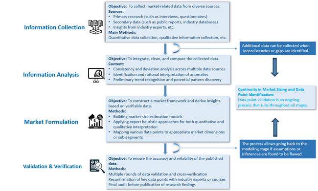
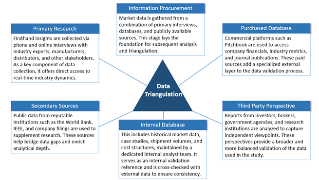
This report offers a comprehensive analysis of the global Lithography Equipment market, examining all key dimensions. It provides both a macro-level overview and micro-level market details, including market size, trends, competitive landscape, niche segments, growth drivers, and key challenges.
Report Framework and Key Highlights:
MarketDynamics: Identification of major market drivers, restraints,opportunities, and challenges.
TrendAnalysis: Examination of ongoing and emerging trendsimpacting the market.
CompetitiveLandscape: Detailed profiles and market positioning of majorplayers, including market share, operational status, product offerings, andstrategic developments.
StrategicAnalysis Tools: SWOTAnalysis, Porter’s Five Forces Analysis, PEST Analysis, Value Chain Analysis
MarketSegmentation: By type, application, region, and end-userindustry.
Forecastingand Growth Projections: In-depth revenue forecasts and CAGRanalysis through 2033.
This report equips readers with critical insights tonavigate competitive dynamics and develop effective strategies. Whetherassessing a new market entry or refining existing strategies, the report servesas a valuable tool for:
Industry players
Investors
Researchers
Consultants
Business strategists
And all stakeholders with an interest or investmentin the Lithography Equipment market.
Global Lithography Equipment Market:Segmentation Analysis and Strategic Insights
This section of the report provides an in-depthsegmentation analysis of the global Lithography Equipment market. The market issegmented based on region (country), manufacturer, product type, andapplication. Segmentation enables a more precise understanding of marketdynamics and facilitates targeted strategies across product development,marketing, and sales.
By breaking the market into meaningful subsets,stakeholders can better tailor their offerings to the specific needs of eachsegment—enhancing competitiveness and improving return on investment.
Global Lithography EquipmentMarket: Market Segmentation Analysis
The research report includes specificsegments by region (country), manufacturers, Type, and Application. Marketsegmentation creates subsets of a market based on product type, end-user orapplication, Geographic, and other factors. By understanding the marketsegments, the decision-maker can leverage this targeting in the product, sales,and marketing strategies. Market segments can power your product developmentcycles by informing how you create product offerings for different segments.
|
ATTRIBUTE |
Details |
|
|
Time Coverage |
Historical Year: 2020– 2024 Base Year: 2024 Estimated Year: 2025 Forecast Year: 2025 - 2033 |
|
|
Market Segmentation |
||
|
By Type |
EUV ArFi ArF KrF i- line Others |
|
|
By Application |
Advanced Packaging LED MEMs Power Devices Others |
|
|
By Company |
ASML Holding NV Nikon Corporation Canon Inc. Shanghai Micro Electronics Equipment (SMEE) EV Group Veeco Instruments Inc. JEOL Ltd. Onto Innovation Inc. SÜSS MicroTec NuFlare Technology |
|
|
By Region |
North America |
|